- 您现在的位置:买卖IC网 > Sheet目录323 > DS3050W-100# (Maxim Integrated)IC NVSRAM 4MBIT 100NS 256BGA
�� �
�
�3.3V� Single-Piece� 4Mb� Nonvolatile� SRAM�
�with� Clock�
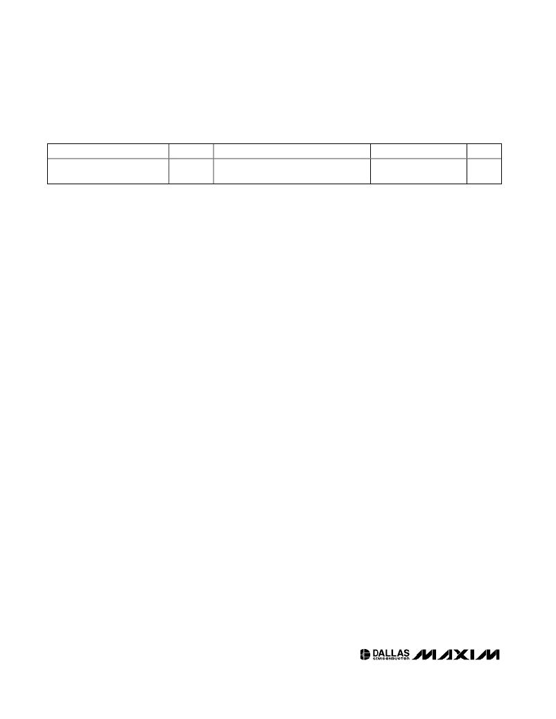
�DATA� RETENTION�
�(T� A� =� +25� °� C.)�
�PARAMETER�
�Expected� Data-Retention� Time�
�(Per� Charge)�
�SYMBOL�
�t� DR�
�(Notes� 7,� 8)�
�CONDITIONS�
�MIN�
�2�
�TYP�
�3�
�MAX�
�UNITS�
�Years�
�AC� TEST� CONDITIONS�
�Input� Pulse� Levels:�
�Input� Pulse� Rise� and� Fall� Times:�
�Input� and� Output� Timing� Reference� Level:�
�Output� Load:�
�V� IL� =� 0.0V,� V� IH� =� 2.7V�
�5ns�
�1.5V�
�1� TTL� Gate� +� C� L� (100pF)� including� scope� and� jig�
�Note� 1:�
�Note� 2:�
�Note� 3:�
�Note� 4:�
�Note� 5:�
�Note� 6:�
�Note� 7:�
�Note� 8:�
�Note� 9:�
�Note� 10:�
�Note� 11:�
�Note� 12:�
�Note� 13:�
�IRQ� /FT� and� RST� are� open-drain� outputs� and� cannot� source� current.� External� pullup� resistors� should� be� connected� to� these�
�pins� to� realize� a� logic-high� level.�
�These� parameters� are� sampled� with� a� 5pF� load� and� are� not� 100%� tested.�
�t� WP� is� specified� as� the� logical� AND� of� CE� with� WE� for� SRAM� writes,� or� CS� with� WE� for� RTC� writes.� t� WP� is� measured� from�
�the� latter� of� the� two� related� edges� going� low� to� the� earlier� of� the� two� related� edges� going� high.�
�t� WR1� and� t� DH1� are� measured� from� WE� going� high.�
�t� WR2� and� t� DH2� are� measured� from� CE� going� high� for� SRAM� writes� or� CS� going� high� for� RTC� writes.�
�t� DS� is� measured� from� the� earlier� of� CE� or� WE� going� high� for� SRAM� writes,� or� from� the� earlier� of� CS� or� WE� going� high� for�
�RTC� writes.�
�In� a� power-down� condition,� the� voltage� on� any� pin� may� not� exceed� the� voltage� on� V� CC� .�
�The� expected� t� DR� is� defined� as� accumulative� time� in� the� absence� of� V� CC� starting� from� the� time� power� is� first� applied� by� the�
�user.� Minimum� expected� data-retention� time� is� based� upon� a� maximum� of� two� +230� °� C� convection� reflow� exposures,� fol-�
�lowed� by� a� fully� charged� cell.� Full� charge� occurs� with� the� initial� application� of� V� CC� for� a� minimum� of� 96� hours.� This� parame-�
�ter� is� assured� by� component� selection,� process� control,� and� design.� It� is� not� measured� directly� during� production� testing.�
�WE� is� high� for� any� read� cycle.�
�OE� =� V� IH� or� V� IL� .� If� OE� =� V� IH� during� write� cycle,� the� output� buffers� remain� in� a� high-impedance� state.�
�If� the� CE� or� CS� low� transition� occurs� simultaneously� with� or� latter� than� the� WE� low� transition,� the� output� buffers� remain� in� a�
�high-impedance� state� during� this� period.�
�If� the� CE� or� CS� high� transition� occurs� prior� to� or� simultaneously� with� the� WE� high� transition,� the� output� buffers� remain� in� a�
�high-impedance� state� during� this� period.�
�If� WE� is� low� or� the� WE� low� transition� occurs� prior� to� or� simultaneously� with� the� related� CE� or� CS� low� transition,� the� output�
�buffers� remain� in� a� high-impedance� state� during� this� period.�
�4�
�_____________________________________________________________________�
�发布紧急采购,3分钟左右您将得到回复。
相关PDF资料
DS3065W-100#
IC NVSRAM 8MBIT 100NS 256BGA
DS3065WP-100IND+
IC SRAM 3.3V 8MB 34POWERCAP MOD
DS3070W-100#
IC NVSRAM 16MBIT 100NS 256BGA
DS321X
KIT X-WIDE DESIGN STRIP VERT
DS323X
KIT X-WIDE DESIGN STRIP VERT
DS87001-E52
ADAPTER MCU 52-TQFP TO 40-DIP
DS89C450-K00
EVAL KIT FOR DS89C450
DSP56311EVM
KIT EVALUATION FOR DSP56311
相关代理商/技术参数
DS30519
制造商:DIODES 制造商全称:Diodes Incorporated 功能描述:2.0A SURFACE MOUNT SCHOTTKY BARRIER RECTIFIER
DS305710A
制造商:Amphenol Corporation 功能描述:
DS305710A(621)
制造商:Amphenol Corporation 功能描述:
DS305712A
制造商:Amphenol Corporation 功能描述:
DS305712A(621)
制造商:Amphenol Corporation 功能描述:
DS305716A
制造商:Amphenol Corporation 功能描述:
DS305716A621
制造商:Amphenol Corporation 功能描述:
DS30574A
制造商:Amphenol Corporation 功能描述: